THOR & qRICO technology
working principles and advantages
THOR technology

See details for THOR patent here:
https://patents.google.com/patent/WO2020011560A1/en
Our advanced Raman microscopes THOR based on mirrorless Raman beam delivery technology ideally suited for most sophisticated applications in Raman microscopy:
- fast 3D Raman imaging;
- SERS imaging;
- polarised Raman imaging;
- low frequency Raman measurements;
- stokes/antistokes Raman measurements;
- fast optical shutter technology (<1ms).THOR can be upgraded for quantitative Raman based crystallographic orientation mapping (qRICO technology). We develop qRICO technology in collaboration with our partner Xnovo Technology ApS. THOR and qRICO technology covered by 4 international patents licensed by Lightnovo. Based on our collaboration setup, Lightnovo develops and manufactures qRICO devices, support it with polarized Raman data acquisition and data analysis software. Xnovo Technology develops crystallographic data reconstruction and crystallographic data analysis software. Xnovo Technology also responsible for commercialization and sales of qRICO solution. Please contact Xnovo Technology for the price offer regarding qRICO solution: https://xnovotech.com/
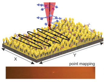
Wide Line Surface‐Enhanced Raman Scattering (WL-SERS) Mapping
The main blocks for WL‐SERS are the following:
- (i) Laser beam delivery system where the laser point focus, diffraction limited line and wide line laser illumination modes are implemented.
- (ii) Epi‐detection‐based microscope for simultaneously obtaining an optical image and a laser beam illumination profile on the surface of the SERS substrate.
- (iii) Raman beam delivery system capable of projecting an aberration‐corrected laser line image onto a spectroscopic imaging sensor.
Laser Beam Delivery
The laser beam delivery layout consists of two geometries: the first geometry is a point illumination mode and the second geometry is for producing the DLL and WL sample illumination modes. The DLL‐focus mode is achieved when a sample is illuminated by a diffraction limited laser line, that is, dDLL = 2.8 µm in width using a 785 nm laser excitation wavelength and 10× magnification lens. The WL mode is obtained by expanding the width of the laser line, that is, dWL> 2.8 µm and up to 64 µm, which is achieved by adjusting the position of a cylindrical lens in the laser delivery path. The laser beam profile is modified using a set of cylindrical lenses including laser line generator lens.
In order to image the entire ≈2 mm long DLL/WL laser profile on a sample, the aperture for the laser beam was designed to fit the field of view (FOV = 2.2 mm) of the 10× near‐infrared (NIR) microscope objective.
Microscope Construction
The sample surface is imaged by a camera while collecting SERS spectra, which simplifies the measurement procedure. This was realized by combining the incident laser beam with visible light from a light emitting diode (LED). To ensure that the white light source is not contributing to the recorded SERS spectra in the 785–1000 nm wavelength range, the NIR emission from the LED source was suppressed (on the order ≈106) by an edge filter.
The camera projection optics is designed to enable imaging of the entire microscope objective FOV with a homogeneous sample illumination. This is usually not the case for most commercial Raman microscopes that only utilize the central part of FOV.
Raman Beam Delivery
The optical path from sample to spectrograph slit is designed to transmit an aberration‐free image of the DLL or WL laser profile. This is achieved by combining a low numerical aperture (NA) collimating lens with a high NA focusing lens in the imaging spectrograph. The low NA collimating lens allows one to insert the lens with equal NA. Therefore, the focal length of the pre-slit lens is sufficiently long for delivering the DLL/WL image from the sample surface to the slit, and with correct input angles at the spectrometer. In this way, beam cutting inside the spectrograph is avoided. Alternatively, the image delivery can be obtained using two intermediate lenses between a microscope objective and a lens; however, this leads to losses in the Raman signal and increases aberrations.
Due to the low NA of the slit and collimating lenses, even at dslit = 100 µm slit, the pixel size limited spectral resolution is ≈1.8–2.5 cm−1 throughout the Raman Stokes shift range of 350–2200 cm−1.
qRICO technology

Currently, crystallographic imaging can be done with three methods: X-ray, electron or neutron diffraction. All these technologies require very expensive equipment (~1.5M€), specialised laboratories, intricate sample preparation and are limited either in spatial resolution or 3D sample mapping, even in their most sophisticated realisations. Nevertheless, it is known that the utilisation of visible light can be used for the determination of crystal orientation. However, nobody has actually been successful in the realisation of quantitative orientation analysis – until now. Lightnovo’s technology, called qRICO, is capable of performing 2D and 3D orientation mapping of materials as precise as electron microscopy. The underlying patented approach of Lightnovo’s technology solves the shortcomings of current methods, providing qRICO with the potential to replace today’s conventional approaches of crystallographic imaging in many areas
Benefits from uniquely differentiated qRICO technology:
- no sample preparation
- no limitation on sample area
- high resolution (200nm)
- fast mapping (0.5-2 ms per point)
- non-destructive 3D orientation mapping
- device cost (up to 3-4x lower)
- compact size & variable footprint
- modular design
To be confident in accuracy of a our new method, we compared orientation map of polycrystalline silicon sample obtained with qRICO technology (Figure a) with the map of the same sample area obtained using electron backscatter diffraction (EBSD) technique (Figure b). A map of the local orientation difference (misorientation angle) exhibits an average orientation difference of ~2.1° (Figure c). We argue that this error is dominated by a geometrical distortions appeared in EBSD data. In order to minimise this effect we corrected the EBDS map for distortions and removed grain boundaries. Artifact which are still present on the map (Figure c) may be connected with orientation-dependent ambiguity of qRICO method and an orientation determination error of EBSD. Overall accuracy of qRICO method is comparable to widely-used EBSD technique.